Small is beautiful: Why ultra precision manufacturing is such a big deal
Are you happy with your smartphone? Bill O’Neill, Professor of Laser Engineering and Director of the IfM’s Centre for Industrial Photonics isn’t.
In fact, he is rather dismissive of the current crop with their basic satellite navigation and camera functionality. Instead, he is contemplating the next generation of ‘personal assistants’ which will be able to monitor your heart rate, tell you how much alcohol you have in your bloodstream or give you a complete check-up by analysing the chemistry of your sweat. This phone will have a whole array of miniature sensors and microprocessors embedded in it derived from the latest breakthroughs in microelectromechanical systems (MEMS) technology.
But to make devices like these requires extraordinary levels of precision – the ability to manufacture intricate features that are smaller than 100 nanometres. To put that number into perspective, a human hair is comparatively huge at somewhere between 50,000 to 100,000 nanometres in diameter. Diagnostic smartphones are just one example of the new kinds of products that are going to need ultra precision manufacturing. The emergence of carbon-based or polymer semiconductor materials like graphene is driving research and development in areas such as the production of lower cost, more efficient solar cells and ‘printed electronics’ that can be used for flexible display screens and smart labelling. These have the potential to be created cheaply and in very large volumes but if that is to become a reality, companies are going to need a whole new set of production capabilities.
The ultra precision research carried out by Bill O’Neill and his team at the IfM is focused on building these kinds of machines and developing the associated systems and processes that can make things at these nano levels of precision. The team works in close collaboration with other researchers across the University of Cambridge who are experts in the new materials and are developing new devices based around them.
Having done so much of the materials research in this country, we need to capitalise on it by creating production-level competencies. If we don’t invest in this now, we’ll end up without a significant foothold in production.
|
|
|
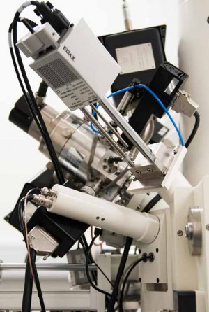
Focused Ion Beam (FIB) microscope which can image and machine materials at a scale of 10nm. |
As Bill is quick to emphasise, it is critical for the UK economy that we invest in the manufacturing capabilities as well as doing the baseline research. “Having done so much of the materials research in this country, we need to capitalise on it by creating production-level competencies. If we don’t invest in this now, we’ll end up without a significant foothold in production. This was exactly what happened with semiconductors even though the UK carried out much of the underlying research in the 1960s. We can’t allow the same thing to happen with the polymer electronics industry and the new opportunities that are coming with carbon and graphene science. This is the case we put to the government.”
And the UK government has clearly listened. In 2011, the Engineering and Physical Sciences Research Council (EPSRC) awarded funding of £6 million to the Centre for Innovative Manufacturing in Ultra Precision, a joint venture between the University of Cambridge and Cranfield University. The collaboration with Cranfield is an important one, which builds on the respective expertise of the two institutions.
“Cranfield has decades of experience of designing machines, including some of the most precise machine tools in the world. By virtue of the extensive materials research taking place across the University (in particular at the Centre for Advanced Photonics and Electronics (CAPE) and the Department of Materials Science), the Cambridge team has had much more experience of working with the new generation of unconventional semiconductor materials. We also have laser and focused ion machinery so can provide new energy sources for processing materials. The partnership with Cranfield coupled with the cross-Cambridge collaborations creates a very strong team with the potential to transform the way we think about and make the next generation of products.”
The research carried out by the Centre is focused on three key areas. The first is looking at ‘roll-to-roll’ printed electronics which, as the name implies, is a process whereby conductive inks are printed onto rolls of plastic, optical film and other flexible materials. This process promises mass production at a fraction of the cost of producing conventional electronics and the ability to print onto large and flexible materials has obvious benefits for things like display systems.
The second research area is based around more conventional machine systems but ones which can produce very precise mechanical components with accuracies of a few tens of nanometres. At the moment these machines are huge but the new systems being designed at Cranfield are very compact with extremely high levels of accuracy and efficiency.
Thirdly, the IfM team is developing a hybrid of focused ion beam and laser technology. At the moment, semiconductor materials are usually processed using focused ion beams (FIBs) but the process is a slow one. By combining a FIB system with laser technology, its efficiency will be increased by three orders of magnitude, transforming what was a high precision but low productivity system into a high precision and high productivity system. It will be able to deal with high volume additive and subtractive manufacturing processes using a wide range of the new semiconductor materials with a resolution down to, in the first instance, 30 nanometres.
These three research ‘platforms’ are focused on developing the underlying machine capability. Over and above these are a growing number of research projects looking at the devices these machines can make and how the new materials they are working with respond to these production processes.
 |
|
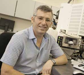
Professor Bill O'Neill |
The Centre benefits from the involvement of industrial research partners including Carl Zeiss, Jaguar Land Rover, Oxford Instruments and the National Physical Laboratory. Working with industry and building a much bigger, highly connected ultra precision community to help develop a fully fledged manufacturing capability in the UK is one of the Centre’s key aspirations. One of the obstacles it needs to overcome is that a lot of companies using ultra precision processes and equipment do not consider themselves to be within the ultra precision ‘sphere’. The Centre has started a national outreach programme to raise the profile of ultra precision with the aim of creating an effective national hub for industry and academia where knowledge and resources can be shared to mutual advantage.
As Bill describes it: “The endgame for us is to provide industry with a wide range of experts in various disciplines that are centred around the design, development and production of ultra precision products and processes.” And also, apparently, to get a better phone.
Key industrial partners include:
- Aerotech
- AIXTRON
- ALE
- Carl Zeiss
- Cranfield Precision Engineering
- Hexagon
- IPG Lasers
- Jaguar Land Rover
- Michell Instruments
- Oxford Instruments
- National Physical Laboratory
- SPI Lasers
Investing in the future
The EPSRC Doctoral Training Centre in Ultra Precision Manufacturing
As part of the initiative to develop an ultra precision skills base, the EPSRC has invested a further £6 million in a centre for doctoral training (CDT), also jointly run by Cranfield and Cambridge. Students at the CDT take a one-year Masters of Research (MRes) followed by a three-year PhD. For UK students and EU students who have studied full-time for three years in the UK, the EPSRC provides full funding and industrial sponsors offer additional financial support during the PhD phase. The CDT welcomed its first intake of students in 2012. Recruitment is under way for the 2014 cohort.


