The use of ultrafast laser annealing to remove ion beam implanted gallium
Introduction
Technology is rapidly progressing towards smaller devices that offer greater functionality at lower prices than previous generation devices. Examples of this trend could be cited from the mobile phone industry, portable music players or computer hardware development. Regardless of the sector, if this trend is to continue, the means to manufacture smaller and more complex devices is likely to be of critical importance in the near future.
One important manufacturing tool is the Focused Ion Beam, or FIB. The FIB allows for ultra-precise deposition, milling and implantation of material, with a resolution of the order of tens of nanometers. Current applications include TEM sample preparation, MEMS prototyping, nanoembossing stamp manufacture, FIB maskless lithography and many other more. For most FIB applications, gallium is the ion of choice:
- Gallium has a low melting point and low volatility. As such it can be kept in the liquid phase easily at just above room temperature and stored for long periods of time without appreciable material loss
- A high brightness can be achieved as the gallium source is liquid, which combined with a fine, sharp tip, leads to ionization and field emission of the ions
- The atomic mass of gallium is sufficiently high to give an acceptable sputter yield, which defines the milling rate, of high atomic mass substrates, while not being too high to cause excessive subsurface damage to low atomic mass substrates
When the accelerated ions collide with a substrate, the ions undergo a series of elastic and inelastic collisions with substrate atoms before coming to rest within the material, where they remain implanted. These collisions also create other lattice defects and can lead to the build up of an amorphous layer in crystalline substrates. The implantation of gallium causes many changes in material properties, such as electrical conductivity or surface hardness, which may in turn impair device function. Due to this, the scope of FIB manufacturing is limited.
Aims & Objectives
The work being carried out investigates a novel method of removing implanted gallium by use of ultrafast laser annealing. The ongoing aims of this investigation are to:
- Validate the process of ultrafast laser annealing for removal of FIB implanted gallium in amorphous and crystalline substrates
- Investigate the effects of laser pulse fluence, wavelength and pulse duration on the migration of FIB implanted gallium
- Form a model of the ultrafast annealing process describing the migration of gallium
- Optimize annealing conditions for maximum removal of implanted gallium
- Assessment of effects of annealing on any structural features created using FIB
Ultrafast laser annealing
The process of ultrafast laser annealing is thought to function as follows - Ultrafast laser pulses, with duration of the order of a few hundred femtoseconds, below the damage threshold of the material, are used to induce a localized ultrafast melt phase. During this phase gallium is able to diffuse out of the material along a concentration gradient. Once the laser energy is removed, the substrate re-solidifies, with lattice structure regained based on liquid phase epitaxial regrowth.
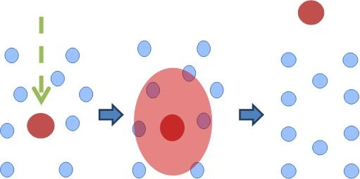
Figure 1 - Schematic of ultrafast laser annealing process. Ultrafast laser pulse (green) is absorbed by material (blue) and implanted gallium (red). This generates an ultrafast melt phase, during which the gallium diffuses out of the material. The substrate then reforms based on liquid phase epitaxial re-growth.
Ultrafast laser annealing offers several advantages over conventional thermal and longer duration laser annealing.
- Due to the timescale of the laser pulse, energy cannot be dissipated thermally, and as such all changes are confined to the focal volume of the laser. This allows for precision annealing, and permits annealing of devices containing thermally or optically sensitive components.
- The high peak power associated with ultrafast laser pulses means the pulse energy required for modification may be significantly less than that for longer duration pulses, making the process more energy efficient.
- As the absorption mechanism is non-linear, the energy may be deposited in small focal volumes near the surface, which permits for annealing of materials normally transparent at the laser wavelength, or for surface annealing of materials with a long absorption length. This is of importance as most of the implanted gallium is located within a few hundred nanometers of the surface, allowing for larger quantities to be removed.
The study is initially focused on glassy carbon and silicon substrates as examples of amorphous and crystalline materials. Relative changes in gallium concentration are measured using kelvin probe force microscopy (KPFM). Initial results, carried out on glassy carbon, show a decrease in surface potential, indicating a decrease in gallium concentration, after annealing the glassy carbon with laser pulses from a Ti:Sapphire laser(wavelength 800 nm, pulse duration 330 fs) at a fluence of 5.4 μJ/cm2.
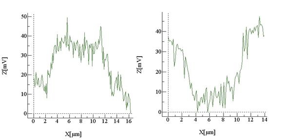
Figure 2 - KPFM profiles of gallium implanted glassy carbon. Left - profile across region implanted at a dose of 3.87 x 10²⁰ ions/cm2. Right - profile along implanted region after ultrafast laser annealing at a fluence of 5.4 μJ/cm2.
Researchers
Funders