Ordered Nanomaterials for Electron Field Emission
Introduction
Field emission has long been studied for the potential in applications such as microwave amplifiers, travelling wave tubes, electron microscopy, and x-ray sources. This project focuses primarily on x-ray applications, with the intention of integrating an optimised chip design into a portable x-ray gun towards the end of the project.
Material Comparison
A large meta-analysis of the materials so far used in field emission applications was made. Materials are required to show high maximum current density as well as low turn on electric field to be considered as a promising material in field emission. 1D and 2D materials were shown to have an average turn on field half the size of 3D/bulk materials. The best performing group of materials were the nanocarbons including carbon nanotubes, graphene, carbon nanowalls and carbon nanofibers.
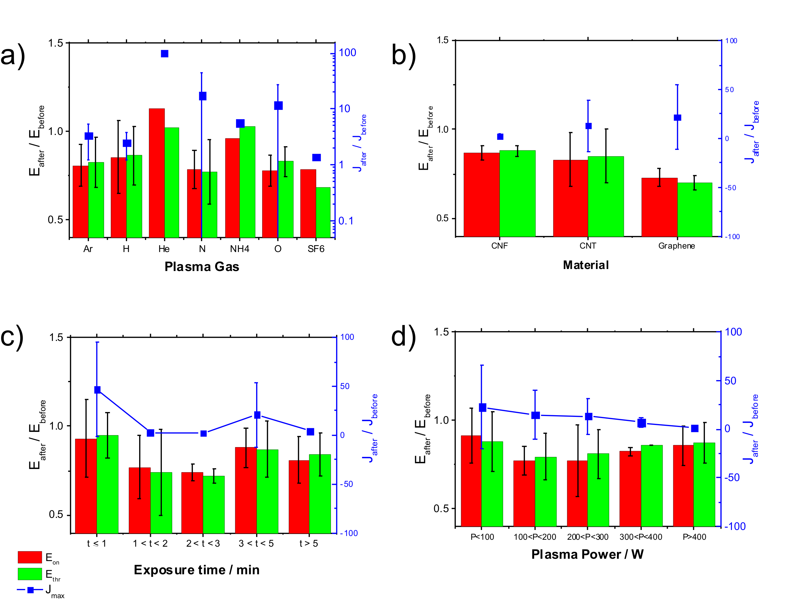
Plasma Etching on Graphitic Nanocarbons
The effect of plasma etching on the graphitic nanocarbons was performed. Plasma etching improves the field emitting capabilities of these materials. The factors taken into consideration were gas etchant used, material, exposure time and plasma operating power. It was found that the best performance was shown by graphene, using a nitrogen plasma at a power between 100 W and 200 W for between 1 and 2 minutes.
Experimental Section
Current experimental work focuses on field emission from carbon nanotube emitters. Integral to the designs are differences in surface morphology, with the hope of discovering a link between emitter geometry and field emission performance. 52 different emitter designs with differences in shape, size and height have begun to be tested. A custom built Scanning Anode Field Emission Microscope is used to measure the field emission performance of the emitters. A base pressure of the order 10-7 mbar is used at room temperature. A tungsten tip with diameter 100 nm is held above the sample at distances controlled by a piezo stage. I-V sweeps are performed from 0 – 1100 V using a source measurement unit (Keithley 237). A raster scan of the emitter builds up a planar picture, piezo stages are also used in the x-y plane with a minimum step size of 40 nm. Analysis of these maps will indicate the best emitter geometry and the designs can be optimised.

Publications
R. J. Parmee, C. M. Collins, W. I. Milne, & M. T. Cole, X-ray generation using carbon nanotubes, Nano Conv., 2, 1, 2015.