Femtosecond Laser Processing of Graphene for Device Applications
Introduction
Graphene is a single atomic carbon arranged in hexagon, firstly discovered in 2004. During the last decade, graphene has attracted enormous interest, emerging as an exciting new material with the potential to impact many areas of basic research and technology [1-3]. Graphene has potentially useful electronics properties, but it is difficult to pattern graphene in different geometry for devices. Although conventional lithography methods can provide precisely located nano/micro patterning and cutting on graphene, it involves a long sequence of process operations, which may also increase the risk of contamination. Femtosecond laser micromachining has the potential for offering free-form post-patterning of general graphene devices with limited thermal effects, high processing speed and complex shapes.
Objectives
The aim of this project is to investigate the capabilities of high-precision laser profiling of monolayer graphene as a device manufacturing step. To achieve this, the central aim of this work is separated into two distinct objectives:
- Understand the underlying physics of the mechanism of ultrafast laser pulse interaction with single layer graphene during the ablation process.
- Based on the theoretical, experimental work will be carried out to allow optimization of cutting parameters.
Success of this project will deliver a new manufacturing route for graphene based devices such as sensors, transistors and solar cells.
Progress
In our process, the single-pulse fluence range was determined to be 66 mJ/cm2~120 J/cm2, in which the selective removal of graphene was achieved without damaging the silicon substrate. SEM images revealed high quality cuts (standard deviation 40 nm) with little damage and re-deposition. Raman maps showed no discernable laser induced damage in the graphene close to the ablation zone. Atomic force microscopy (AFM) revealed an edge step height ranging from less than 2 nm to 10 nm, suggesting little removal of SiO2 and no damage to the silicon (the central path showing sub ablation threshold swelling). This could because that the absorption of Si are higher than graphene though below their damage threshold at near infrared. The effect of the ultrafast laser on the surface potential at the cut edge has been measured. Subthreshold process can induce defects in graphene and the defects were analysed by Raman spectroscopy. This could provide a new way to functionalise graphene for biosensor applications.
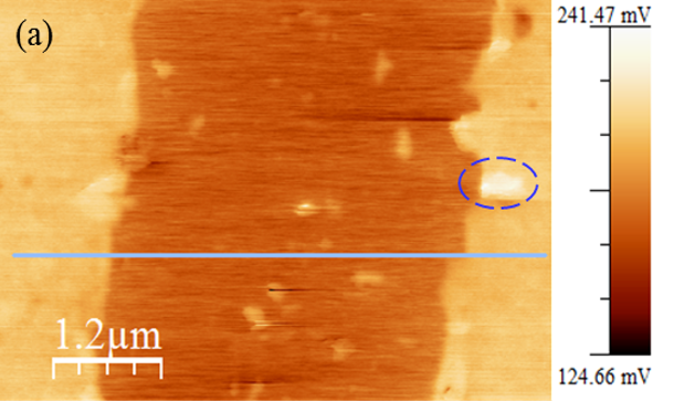
Kelvin probe force microscopy (KPFM) surface potential map of the cut kerf shown at the edge where the graphene flake has folded over itself to create bilayer graphene is indicated by the dashed circle, having a higher CPD than the monolayer graphene
Researchers